
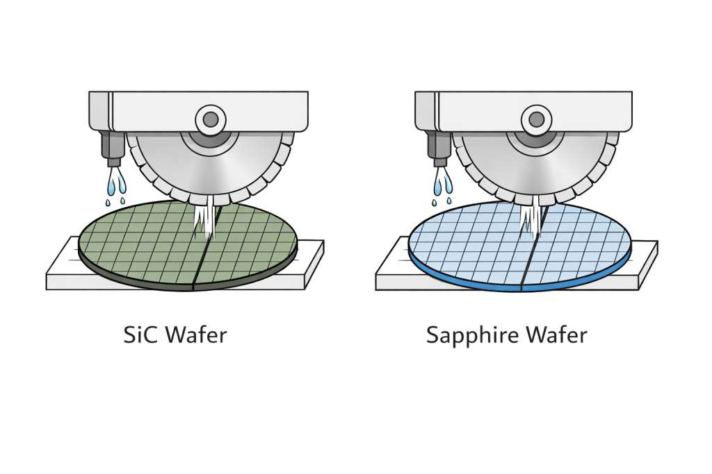
Silicon carbide (SiC) and sapphire wafers are critical materials in modern electronics and optoelectronics due to their exceptional thermal, mechanical, and optical properties. SiC powers high-voltage devices and electric vehicles, while sapphire is widely used in LED substrates and optical windows. However, the superior hardness and brittleness of these materials present unique challenges during wafer processing, particularly during the dicing stage. Precision dicing saws play an indispensable role in ensuring high yield, minimal damage, and optimal device performance.
Understanding the Challenge
SiC and sapphire are among the hardest materials used in semiconductor and optical industries. SiC ranks 9 on the Mohs hardness scale, while sapphire (single-crystal aluminum oxide, Al₂O₃) reaches a similar level of hardness. Their high hardness makes conventional cutting methods ineffective, and their brittleness increases the risk of cracking, chipping, and surface damage during mechanical processing.
Dicing wafers into individual chips or dies is a critical step that requires precise control over cutting depth, feed rate, and blade quality. Any imperfections introduced at this stage can propagate into device failure, reducing yield and increasing manufacturing costs.
Role of Precision Dicing Saws
Precision dicing saws are specialized machines designed to cut hard and brittle wafers with micron-level accuracy. Key features that make them essential include:
- Ultra-High-Precision Motion Control
Modern dicing saws employ linear motors and high-resolution encoders to control the wafer movement with sub-micron accuracy. This precision minimizes kerf width variations and ensures consistent die dimensions. - Optimized Blade Selection
Diamond-coated blades are typically used for SiC and sapphire dicing due to their superior hardness and wear resistance. Blade design, grit size, and bonding type are carefully selected based on wafer thickness and material properties to reduce chipping and micro-cracks. - Controlled Cutting Parameters
Feed rate, spindle speed, and water flow for cooling are precisely regulated to balance cutting efficiency and material integrity. Excessive speed or force can lead to thermal or mechanical stress, while insufficient cutting pressure reduces throughput. - Minimal Damage and Surface Quality
Precision saws reduce subsurface damage, a crucial factor for high-power SiC devices and optical sapphire applications. A smooth cut edge ensures reliable electrical contact, proper die alignment, and optical clarity.
Benefits for SiC and Sapphire Device Manufacturing
- Improved Yield: Reducing chipping, cracking, and micro-fractures minimizes wafer loss and enhances overall yield.
- Enhanced Device Performance: Smooth die edges and minimal subsurface damage improve electrical performance for SiC power devices and optical performance for sapphire components.
- Cost Efficiency: High-precision dicing reduces the need for rework, cleaning, or polishing, optimizing production costs.
- Compatibility with Advanced Packaging: Precision cuts support fine-pitch designs and high-density packaging trends in both electronics and photonics industries.
Future Trends
With the industry shift toward larger wafer diameters—such as 6-inch to 8-inch SiC wafers and high-volume sapphire substrates—precision dicing saws must evolve to handle larger, thinner, and more fragile wafers. Developments include:
- Laser-assisted dicing: Combining mechanical and laser techniques to reduce stress.
- Automated inspection: Integrating real-time monitoring to detect cracks or blade wear.
- Advanced blade materials: Ultra-dense diamond composites and coated ceramics for extended blade life.
Заключение
Precision dicing saws are more than just cutting tools—they are critical enablers of high-performance SiC and sapphire device manufacturing. By providing controlled, accurate, and low-damage wafer separation, these machines ensure device reliability, improve yield, and support the growing demands of power electronics, LEDs, and optical applications. As wafer sizes increase and device architectures become more complex, the role of precision dicing saws will become even more pivotal in the semiconductor and optoelectronic industries.