
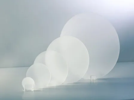
Sapphire (Al₂O₃) substrates are essential materials in modern optics, electronics, and LED industries due to their exceptional hardness, thermal stability, and optical transparency. Achieving high-purity sapphire substrates involves precise control of crystal growth, orientation, and surface finishing. This article provides an overview of the main manufacturing methods, including the Kyropoulos (KY) and Edge-defined Film-fed Growth (EFG) techniques, as well as the subsequent polishing workflow.
Crystal Growth Methods
Kyropoulos (KY) Method
The Kyropoulos method is a slow crystal growth technique that produces large, high-quality sapphire boules with minimal defects. In this process, a seed crystal is immersed into molten high-purity alumina and slowly pulled upwards while carefully controlling temperature gradients. This method favors uniform crystal structure, low dislocation density, and high optical clarity, making it ideal for substrates used in high-performance optics and semiconductor devices.
Advantages of KY Method:
- Large-diameter crystals (up to 12 inches or more)
- Excellent optical uniformity and low internal stress
- High structural integrity suitable for demanding applications
Edge-defined Film-fed Growth (EFG) Method
The EFG method is a faster and more cost-effective approach, particularly for producing thin, wafer-shaped sapphire substrates. In this technique, molten alumina is guided through a shaped graphite die, which defines the crystal’s cross-section. The crystal grows as it is slowly pulled from the die, forming a continuous ribbon or wafer.
Advantages of EFG Method:
- Efficient production of thin, uniform wafers
- Flexible shapes and sizes using different die designs
- Lower production costs compared to KY for certain wafer sizes
Polishing Workflow
After crystal growth, sapphire substrates undergo a rigorous polishing process to achieve the optical-grade flatness and surface smoothness required for advanced applications. The workflow typically includes the following stages:
- Cutting and Shaping:
Large sapphire boules are sliced into wafers using wire saws. The orientation of the crystal (c-plane, a-plane, or r-plane) is carefully considered for subsequent device applications. - Lapping:
Wafers are ground against a flat reference surface with abrasive slurry to remove saw marks and achieve uniform thickness. - Chemical-Mechanical Polishing (CMP):
CMP combines chemical etching with mechanical polishing to produce nanometer-scale surface roughness. Slurries containing fine abrasives and reactive chemicals are used to remove subsurface damage while preserving crystal integrity. - Final Inspection:
Polished wafers are examined for flatness, thickness variation, and surface defects. Advanced metrology tools ensure that substrates meet strict specifications for optical and electronic applications.
Applications and Significance
High-purity sapphire substrates are widely used in LEDs, semiconductor devices, optical windows, and high-frequency electronics. Their exceptional hardness (Mohs 9), thermal conductivity, and chemical stability make them indispensable in environments where durability and performance are critical. The choice of growth method (KY or EFG) and the precision of the polishing process directly influence substrate quality and device efficiency.
Wnioski
The manufacture of high-purity sapphire substrates is a sophisticated process combining advanced crystal growth and precision surface finishing. Kyropoulos (KY) and Edge-defined Film-fed Growth (EFG) methods each offer unique advantages depending on size, quality, and cost requirements. Coupled with a meticulous polishing workflow, these methods ensure that sapphire substrates meet the stringent demands of modern technology, from optical lenses to high-performance electronics.