
Surface particles are one of the most important cleanliness indicators for semiconductor wafers.
A wafer can meet its requirements for diameter, thickness, TTV, bow, warp, resistivity, and surface roughness while still creating serious manufacturing problems if excessive particles remain on the polished surface.
For semiconductor fabrication, advanced packaging, wafer bonding, epitaxy, thin-film deposition, lithography, and research applications, particle contamination can directly influence process yield.
However, a specification such as “particle count ≤ 20” is incomplete unless the buyer also defines the particle size threshold, inspected area, edge exclusion, inspection equipment, and wafer condition.
This guide explains how semiconductor buyers should evaluate wafer particle size, particle count, particle adders, cleanliness requirements, inspection methods, and incoming inspection criteria.
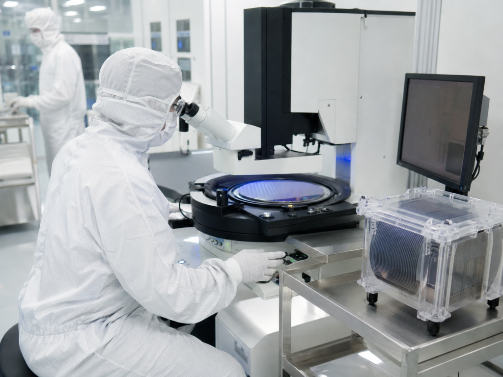
1. Why Wafer Surface Particles Matter
Modern semiconductor processes depend on extremely clean wafer surfaces.
Particles can interfere with subsequent processing in several ways.
Depending on the particle location and process, contamination may cause:
- Lithography defects
- Pattern bridging
- Open circuits
- Short circuits
- Film defects
- Epitaxial defects
- Bonding voids
- Poor adhesion
- Localized etching defects
- Scratches during handling
- Reduced device yield
The importance of particle control becomes even greater as semiconductor features and bonding structures become smaller.
For example, a particle that appears insignificant during basic visual inspection may still interfere with wafer bonding or fine-pitch advanced packaging.
Therefore, wafer cleanliness should be treated as a measurable quality characteristic rather than simply described as “clean.”
2. What Is a Wafer Surface Particle?
A surface particle is a foreign material located on the wafer surface that can be detected by an optical, laser-scattering, or other inspection system.
Possible particle sources include:
- Silicon fragments
- Quartz particles
- Ceramic particles
- Metal contamination
- Polishing residue
- Cleaning residue
- Organic contamination
- Dust
- Packaging debris
- Handling contamination
Particles can be introduced during many manufacturing stages, including:
- Krojenie wafli
- Szlifowanie
- Okrążanie
- Edge processing
- Polerowanie
- CMP
- Czyszczenie
- Kontrola
- Opakowanie
- Transportation
For this reason, particle control must cover the complete wafer manufacturing and handling process.
3. Particle Size Is as Important as Particle Count
When specifying wafer surface particles, particle count alone is not sufficient.
The minimum detectable particle size must also be defined.
A specification might be written as:
Particles ≥ 0.3 μm: ≤ X counts per wafer
or:
Particles ≥ 0.2 μm: customer-defined limit
The principle is important:
A wafer measured using a larger particle-size threshold will normally show fewer particles than the same wafer inspected using a smaller threshold.
Therefore:
10 particles at ≥1.0 μm is not equivalent to 10 particles at ≥0.2 μm.
Whenever a supplier provides particle data, buyers should confirm the detection threshold used for inspection.
4. Common Particle Size Ranges
Different semiconductor applications may focus on different particle size ranges.
Typical inspection discussions may include thresholds such as:
- ≥1.0 μm
- ≥0.5 μm
- ≥0.3 μm
- ≥0.2 μm
- ≥0.1 μm
- Smaller sizes for highly advanced applications
The required detection capability depends heavily on:
- Wafer application
- Device generation
- Sprzęt inspekcyjny
- Wykończenie powierzchni
- Substrate material
- Process sensitivity
A research-grade substrate used for general experiments may not require the same particle performance as a wafer intended for advanced bonding or high-volume semiconductor manufacturing.
Therefore, buyers should avoid copying particle specifications from an unrelated wafer application.
5. What Does Particle Count Mean?
Particle count usually refers to the number of detected particles above a specified size threshold within the defined inspection area.
Na przykład:
Particle count ≥0.3 μm: ≤30 particles/wafer
This specification contains two critical pieces of information:
- Particle size threshold: ≥0.3 μm
- Maximum acceptable count: 30 particles per wafer
However, additional conditions are still required.
The complete specification should ideally also define:
- Średnica płytki
- Inspection area
- Edge exclusion
- Inspection side
- Measurement tool
- Measurement condition
Without these details, particle data from different suppliers may not be directly comparable.
6. There Is No Single Universal Particle Count Limit
One common mistake in semiconductor wafer procurement is asking:
“What is the standard particle count for a semiconductor wafer?”
There is no single number that is appropriate for every wafer.
Acceptable particle count depends on several variables.
Wafer Material
Particle requirements may differ for:
- Krzem
- SOI
- SiC
- Szafir
- GaN
- Szkło
- Kwarc
- Carrier wafers
Wafer Grade
Different expectations may apply to:
- Prime grade
- Epi-ready grade
- Klasa produkcji
- Ocena badawcza
- Test grade
- Klasa manekina
Zastosowanie
Particle requirements may be significantly tighter for:
- Epitaxy
- Hybrid bonding
- Łączenie płytek półprzewodnikowych
- Advanced lithography
than for:
- Equipment testing
- Opracowywanie procesów
- Dummy wafer applications
For B2B wafer purchasing, the particle limit should therefore be agreed according to the final application.
7. Particle Inspection Area and Edge Exclusion
Wafer inspection normally excludes a defined region near the edge.
This region is called edge exclusion.
Possible values may include:
- 1 mm
- 2 mm
- 3 mm
- 5 mm
- Customer-defined edge exclusion
The exact value should be clearly stated in the inspection specification.
This is important because wafer edges may contain:
- Bevel structures
- Edge polishing marks
- Local contamination
- Edge-handling traces
A particle count measured with a 5 mm edge exclusion cannot be directly compared with a count measured using a 2 mm edge exclusion.
For accurate supplier comparison, buyers should request identical measurement conditions.
8. Frontside and Backside Particle Requirements
Particle specifications should also define which wafer surface is being evaluated.
Depending on the wafer, inspection may include:
- Frontside only
- Backside only
- Both sides
The polished device surface normally receives the strictest control.
However, backside cleanliness can also be important.
Backside particles may cause:
- Chucking problems
- Wafer tilt
- Handling instability
- Local stress
- Cross-contamination
- Lithography focus problems
For advanced processing, buyers may therefore need separate frontside and backside cleanliness requirements.
9. Laser Scattering Particle Inspection
Laser-based surface inspection systems are commonly used to detect particles and other surface light-scattering events.
The general principle is straightforward.
A laser scans the wafer surface.
Particles or surface irregularities scatter incoming light.
The inspection system detects this scattered signal and estimates the location and size of the detected event.
The resulting inspection data can include:
- Total particle count
- Particle size distribution
- Particle coordinates
- Wafer map
- Defect classification
Automated inspection provides much more useful information than visual inspection alone.
10. Particle Maps Can Reveal Process Problems
A total particle count tells buyers how many particles were detected.
A particle map provides additional information about where those particles are located.
Particle distribution patterns may reveal potential process issues.
Center Concentration
Particles concentrated near the center may indicate a problem associated with:
- Wafer chucking
- Czyszczenie
- Spin processing
Edge Concentration
Particles near the perimeter may indicate:
- Edge handling
- Bevel contamination
- Packaging contact
Repeating Pattern
A repeated geometric pattern may indicate contact with:
- Robot end effectors
- Wafer chucks
- Inspection stages
Random Distribution
Random particles may be associated with:
- Environmental contamination
- Cleaning performance
- Packaging contamination
For supplier qualification, particle maps can therefore provide more useful information than the total count alone.
11. Particle Size Distribution
Instead of specifying only one particle threshold, some buyers may want to review particle size distribution.
For example, inspection data may separate detected particles into different size bins.
This can help distinguish between:
- Large visible contamination
- Medium-size process particles
- Small particle contamination
A wafer containing a few relatively large particles may create different process risks than a wafer containing many smaller particles.
For sensitive processes, particle distribution analysis can therefore support better quality decisions.
12. Particle Adders
Another important concept is particle adders.
Particle adders measure how many additional particles appear after a specific process or equipment step.
A simplified calculation is:
Particle Adders = Particle Count After Process − Particle Count Before Process
Na przykład:
Before processing:
18 particles
After processing:
25 particles
Particle adders:
7 particles
Particle adders are particularly useful when qualifying semiconductor equipment such as:
- Wafer cleaners
- Plasma tools
- Deposition systems
- Etchers
- Wafer handling systems
- Bonding equipment
Instead of judging only the absolute wafer particle count, engineers can determine whether the equipment itself is generating contamination.
13. Pre-Clean and Post-Clean Particle Inspection
Cleaning process qualification often includes particle measurements before and after cleaning.
This helps determine cleaning efficiency.
Na przykład:
Before cleaning: 120 particles
After cleaning: 18 particles
The reduction indicates the effectiveness of the cleaning process.
However, engineers should also consider whether cleaning introduces other defects.
An aggressive cleaning process could reduce particle count while increasing:
- Chropowatość powierzchni
- Chemical contamination
- Stains
- Water marks
- Surface damage
Therefore, particle inspection should be considered together with overall surface quality.
14. Cleanliness Requirements Beyond Particles
A wafer can have a low particle count but still have unacceptable contamination.
Wafer cleanliness may also include control of:
- Metallic contamination
- Organic contamination
- Ionic contamination
- Native oxide
- Surface residue
- Moisture
- Molecular contamination
Different analytical techniques may therefore be required.
Przykłady to między innymi:
- TXRF
- ICP-MS
- XPS
- TOF-SIMS
- Contact angle measurement
- Kontrola powierzchni
Particle inspection should therefore be considered one component of a complete wafer cleanliness program.
15. Metallic Contamination
Metallic contamination can be particularly important for semiconductor device manufacturing.
Possible contaminants include:
- Fe
- Cu
- Ni
- Cr
- Zn
- Al
- Na
- K
Even when such contamination does not appear as an obvious particle, it may still affect semiconductor device performance.
For high-purity semiconductor applications, buyers may therefore request metallic contamination data separately from particle inspection.
16. Surface Roughness vs. Particle Cleanliness
Surface roughness and particle cleanliness are different characteristics.
For example, a polished wafer might have:
Ra ≤0.2 nm
while still containing an unacceptable number of surface particles.
Conversely, a wafer may have low particle counts but fail the required surface roughness specification.
Therefore, incoming wafer quality evaluation should normally treat the following independently:
- Chropowatość powierzchni
- Zadrapania
- Pits
- Liczba cząstek
- Metallic contamination
- Stains
- Wady powierzchniowe
This prevents a wafer from being accepted based on only one surface metric.
17. Particle Requirements for Epi-Ready Wafers
Epi-ready wafers generally require particularly controlled surface conditions because the substrate will be used for subsequent epitaxial growth.
Particle contamination may become a nucleation point for defects during epitaxy.
Epi-ready wafer inspection may therefore consider:
- Liczba cząstek
- Chropowatość powierzchni
- Zadrapania
- Pits
- Zanieczyszczenie powierzchniowe
- Cleaning condition
- Packaging environment
For SiC and other compound semiconductor substrates, surface defects and polishing damage may also need separate characterization.
A low particle count alone does not automatically mean a wafer is suitable for epitaxy.
18. Particle Control for Wafer Bonding
Wafer bonding can be highly sensitive to particles.
When two surfaces are brought together, a particle located between them can prevent intimate contact over a much larger surrounding area.
This may produce:
- Bonding voids
- Reduced bond strength
- Local delamination
- Strata plonu
This is particularly important for:
- Direct wafer bonding
- Hybrid bonding
- SOI manufacturing
- MEMS bonding
- Glass-to-silicon bonding
- Zaawansowane opakowania
As bonding pitch decreases, cleanliness requirements generally become more demanding.
19. Particle Requirements for Advanced Packaging
Advanced packaging introduces additional cleanliness challenges.
Processes may include:
- RDL
- TSV
- TGV
- Fan-out packaging
- Łączenie płytek półprzewodnikowych
- Hybrid bonding
- Tymczasowe łączenie
- Cienienie płytek
Substrates may also become thinner and more fragile.
Particles can interfere with:
- Fine-pitch interconnects
- Bonding interfaces
- Litografia
- Redistribution layers
For these applications, equipment-generated particle adders may be just as important as incoming wafer cleanliness.
20. Packaging Can Affect Final Particle Count
A wafer can leave the cleaning line in excellent condition but become contaminated during packaging.
Do potencjalnych źródeł zanieczyszczeń należą:
- Nośniki płytek
- Cassette surfaces
- FOUPs
- Plastic boxes
- Foam
- Packaging films
- Handling during packing
Semiconductor wafer suppliers should therefore use packaging compatible with the required cleanliness level.
Before approving packaging, buyers may evaluate:
- Carrier material
- Contact points
- Particle shedding
- Cleanroom packaging procedure
- Double-bagging
- Nitrogen packaging where required
Clean manufacturing without clean packaging does not guarantee clean delivery.
21. Transportation and Incoming Inspection
Transportation can introduce additional contamination or wafer movement.
When wafers arrive at the customer’s facility, incoming inspection may verify:
- Stan opakowania
- Wafer quantity
- Wafer identification
- Uszkodzenia krawędzi
- Stan powierzchni
- Liczba cząstek
For critical applications, particle inspection can be compared with the supplier’s outgoing inspection report.
Large differences may indicate problems associated with:
- Opakowanie
- Transportation
- Unpacking
- Local handling conditions
22. Establishing Incoming Particle Acceptance Criteria
A practical incoming specification should contain more information than simply:
Particles ≤20
A better specification structure may include:
Wafer: 200 mm silicon wafer
Inspection side: Frontside
Particle threshold: ≥0.3 μm
Maximum count: Customer-defined limit
Edge exclusion: 3 mm
Inspection: Automated surface particle inspection
The exact values should be adjusted according to application requirements.
For high-value production substrates, buyers may additionally request wafer maps and inspection reports.
23. Supplier Particle Inspection Report
A useful particle inspection report may contain:
- Wafer ID
- Lot number
- Średnica płytki
- Inspection date
- Sprzęt inspekcyjny
- Particle detection threshold
- Total particle count
- Edge exclusion
- Inspection side
- Particle map
- Pass/fail result
For demanding applications, particle size distribution may also be included.
Traceability is especially important when particle-related process problems occur later in manufacturing.
24. Compare Suppliers Using the Same Conditions
Particle specifications are easily misunderstood when comparing suppliers.
Supplier A may report:
8 particles
while Supplier B reports:
15 particles
At first glance, Supplier A appears cleaner.
However, Supplier A may be measuring particles ≥0.5 μm while Supplier B measures particles ≥0.2 μm.
The results are therefore not directly comparable.
When qualifying wafer suppliers, always standardize:
- Particle threshold
- Inspection area
- Edge exclusion
- Sprzęt inspekcyjny
- Wafer side
- Cleaning condition
Only then can particle data be meaningfully compared.
25. Recommended Wafer Particle RFQ Checklist
When requesting semiconductor wafers, buyers can specify:
- Materiał płytki
- Średnica płytki
- Grubość płytki
- Wykończenie powierzchni
- SSP or DSP
- Particle size threshold
- Maximum particle count
- Frontside requirement
- Backside requirement
- Edge exclusion
- Chropowatość powierzchni
- Scratch requirement
- Pit requirement
- Metallic contamination requirement
- Cleaning requirement
- Packaging method
- Particle inspection report
- Wafer map requirement
- Lot traceability
For advanced semiconductor applications, these requirements should ideally be agreed before production.
26. Example Wafer Cleanliness Specification
A procurement specification might be structured as follows:
| Pozycja | Requirement |
|---|---|
| Wafer Material | Silicon / SiC / Sapphire / Customer Specified |
| Średnica płytki | 100–300 mm or Custom |
| Surface | SSP / DSP |
| Particle Threshold | Customer Specified |
| Particle Count | Customer Specified |
| Inspection Side | Front / Back / Both |
| Wykluczenie krawędzi | Customer Specified |
| Chropowatość powierzchni | Application Dependent |
| Particle Map | Optional / Required |
| Czyszczenie | Semiconductor Cleaning |
| Opakowanie | Cleanroom Packaging |
| Inspection Report | Available Upon Request |
The actual limits should be selected according to process requirements rather than using one universal specification.
27. Questions to Ask a Wafer Supplier
Before placing an order, semiconductor buyers should ask:
- What is the minimum particle size your inspection system can detect?
- What edge exclusion is used?
- Is particle inspection performed on every wafer or by sampling?
- Are frontside and backside measured separately?
- Can you provide a particle map?
- What cleaning process is used before final inspection?
- Is inspection performed before or after final packaging?
- Can particle limits be customized?
- Is lot-level traceability available?
- Can you provide outgoing inspection data with the shipment?
These questions help prevent disputes after wafers arrive.
Wnioski
Wafer surface particle inspection is an essential part of semiconductor substrate quality control, but particle count should never be evaluated as an isolated number.
A meaningful cleanliness specification must define particle size threshold, maximum particle count, inspection area, wafer side, edge exclusion, inspection method, and packaging condition.
Particle requirements also vary significantly depending on whether the wafer will be used for research, epitaxy, wafer bonding, advanced packaging, semiconductor manufacturing, or equipment testing.
For buyers, the most important principle is consistency.
Suppliers should be compared using the same inspection threshold and measurement conditions, while incoming inspection criteria should reflect the actual sensitivity of the downstream manufacturing process.
A well-defined particle specification can reduce contamination-related failures, improve supplier qualification, simplify incoming inspection, and ultimately support higher semiconductor process yield.
FAQ
What particle size should be specified for semiconductor wafers?
There is no universal particle-size threshold for every semiconductor wafer. The correct threshold depends on the wafer material, process, device application, and capability of the inspection equipment. Buyers should specify both the particle size threshold and acceptable count.
Is particle count alone enough to determine wafer cleanliness?
No. Particle count should be evaluated together with particle size, inspected area, edge exclusion, wafer side, and measurement conditions. Metallic and organic contamination may also need separate inspection.
What are particle adders?
Particle adders are the increase in particle count caused by a specific process or equipment step. They are usually determined by comparing particle inspection results before and after processing.
Why is particle control important for wafer bonding?
Particles trapped between bonding surfaces can prevent proper contact and create bonding voids. For direct bonding and hybrid bonding, very small particles can affect a much larger surrounding bonding area.
Should particle inspection be included in wafer incoming inspection?
For particle-sensitive semiconductor processes, yes. Incoming inspection can help verify supplier cleanliness, identify shipping or packaging contamination, and prevent contaminated wafers from entering production.
Can semiconductor wafer particle limits be customized?
Yes. Particle size thresholds, count limits, edge exclusion, inspection area, and reporting requirements can be defined according to the customer’s application and quality requirements.