
Wafer bonding has become a cornerstone process in modern semiconductor manufacturing, enabling advanced packaging, MEMS fabrication, heterogeneous integration, and 3D device architectures. As device scaling approaches physical limits and integration complexity increases, wafer-level bonding technologies play an increasingly critical role in achieving high performance, miniaturization, and system-level integration.
Among the various bonding methods available today, direct bonding and anodic bonding are two of the most widely used techniques in research and industrial production. Although both methods achieve permanent wafer-level joining, their physical mechanisms, material compatibility, process conditions, and application domains differ significantly.
This article provides a technical yet accessible comparison of direct bonding and anodic bonding, focusing on process principles, equipment requirements, advantages, limitations, and application scenarios.
1. Fundamentals of Wafer Bonding
Wafer bonding refers to the process of permanently joining two mirror-polished wafers—typically silicon, glass, sapphire, or compound semiconductor substrates—without using intermediate adhesives. The bonding may rely on intermolecular forces, electrostatic attraction, or thermally activated chemical reactions.
The primary objectives of wafer bonding include:
- Enabling 3D integration and wafer stacking
- Fabricating MEMS and microfluidic devices
- Realizing silicon-on-insulator (SOI) structures
- Integrating dissimilar materials
- Enhancing thermal or mechanical performance
High bonding quality requires strict control over:
- Surface flatness and roughness
- Particle contamination
- Alignment accuracy
- Temperature and pressure uniformity
Failure to control these factors can result in voids, delamination, or reduced mechanical strength.
2. Direct Bonding (Fusion Bonding)
2.1 Principle of Operation
Direct bonding, also known as fusion bonding or hydrophilic bonding, relies on atomic-scale interactions between ultra-flat and ultra-clean wafer surfaces.
The bonding process typically involves:
- Surface cleaning and activation (often plasma-assisted)
- Initial room-temperature contact, where van der Waals forces create weak pre-bonding
- High-temperature annealing to strengthen covalent bonds across the interface
For silicon wafers, hydroxyl-terminated surfaces (Si–OH groups) react during annealing to form strong Si–O–Si covalent bonds.
2.2 Process Conditions
- Surface roughness: typically < 0.5 nm RMS
- Cleanroom environment: ISO class 5 or better
- Annealing temperature: 200–1100°C (depending on materials)
- Alignment tolerance: often sub-micron in advanced packaging
2.3 Advantages
- No intermediate adhesive layer
- High bonding strength after annealing
- Excellent thermal and electrical conductivity
- Suitable for high-temperature applications
2.4 Limitations
- Extremely sensitive to particles and surface defects
- Requires ultra-flat wafer surfaces
- High-temperature annealing may induce thermal stress
- Material thermal expansion mismatch must be carefully managed
2.5 Typical Applications
- Silicon-on-insulator (SOI) production
- 3D integrated circuits
- MEMS sensor fabrication
- Advanced power semiconductor packaging
Direct bonding is widely considered a high-precision, high-purity bonding method suitable for advanced semiconductor integration.
3.1 Principle of Operation
Anodic bonding, also called electrostatic bonding, is primarily used to bond silicon to alkali-containing glass (e.g., borosilicate glass).
The process involves:
- Heating the wafer stack (typically 300–450°C)
- Applying a high DC voltage (200–1000 V) across the interface
- Migration of mobile alkali ions (e.g., Na⁺) within the glass
- Formation of a strong electrostatic attraction at the interface
- Chemical bond formation between silicon and oxygen atoms
The result is a hermetic, high-strength bond.
3.2 Process Conditions
- Temperature: 300–450°C
- Voltage: 200–1000 V
- Bonding atmosphere: typically vacuum or controlled environment
- Surface preparation: less stringent than direct bonding
3.3 Advantages
- Lower temperature compared to high-temperature direct bonding
- Strong hermetic sealing
- Tolerant to minor surface imperfections
- Well-suited for silicon-glass integration
3.4 Limitations
- Limited to specific material combinations
- High electric field may induce charge trapping
- Not suitable for all compound semiconductors
- Thermal expansion mismatch must still be considered
3.5 Typical Applications
- MEMS devices
- Microfluidic chips
- Pressure sensors
- Optical packaging
Anodic bonding remains a mature and cost-effective technique for silicon-to-glass applications, particularly where hermetic sealing is critical.
4. Comparative Analysis
| Aspect | Direct Bonding | Anodic Bonding |
|---|---|---|
| Bonding Mechanism | Covalent atomic bonding | Electrostatic + chemical bonding |
| Typical Materials | Si–Si, Si–SiO₂, compound semiconductors | Si–glass |
| Temperature | Moderate to high | Moderate |
| Voltage Required | No | Yes (high DC voltage) |
| Surface Requirement | Extremely high | Moderate |
| Hermetic Sealing | Good | Excellent |
| Equipment Complexity | High precision alignment & annealing | Voltage-controlled bonding system |
From a process integration perspective:
- Direct bonding is preferred for high-performance semiconductor integration and 3D stacking.
- Anodic bonding is optimal for MEMS and sensor packaging requiring glass encapsulation.
5. Equipment Considerations
Both bonding methods require precise equipment engineering.
For Direct Bonding:
- High-precision wafer alignment systems
- Plasma surface activation modules
- Uniform pressure control systems
- High-temperature annealing furnaces
Temperature uniformity and particle control are critical to avoid interfacial voids.
For Anodic Bonding:
- Controlled voltage supply
- Temperature-regulated bonding chamber
- Vacuum capability
- Safety mechanisms for high-voltage operation
Electrical field uniformity significantly affects bonding uniformity and yield.
6. Reliability and Quality Evaluation
Bonding quality is typically evaluated by:
- Infrared imaging for void detection
- Shear strength testing
- Tensile testing
- Hermeticity testing
- Cross-sectional microscopy
In advanced semiconductor manufacturing, process repeatability and defect density are often more important than maximum bond strength alone.
7. Future Trends in Wafer Bonding
As semiconductor devices move toward heterogeneous integration and wide-bandgap materials (such as SiC and GaN), wafer bonding technologies are evolving toward:
- Lower-temperature bonding techniques
- Plasma-assisted and hybrid bonding
- Larger wafer sizes
- Improved alignment precision
- Integration with compound semiconductor materials
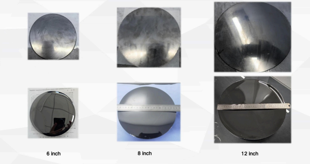
The push toward 12-inch wafer platforms further increases the demand for uniform pressure control and large-area bonding stability.
Conclusie
Direct bonding and anodic bonding represent two fundamentally different yet complementary wafer bonding technologies.
Direct bonding excels in high-purity, high-strength semiconductor integration, while anodic bonding provides reliable hermetic sealing for silicon-to-glass structures. The selection between these methods depends on material compatibility, device architecture, thermal budget, and reliability requirements.
As semiconductor devices continue to scale and diversify, mastering wafer bonding technologies will remain essential for enabling next-generation electronic and microelectromechanical systems.