


 Ultra-Thin Free-Standing Diamond Film is an innovative thermal management material specifically designed for advanced semiconductor packaging, high-power electronics, and emerging photonic systems.
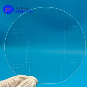
Manufactured using advanced MPCVD diamond growth technology, the film features a self-supporting polycrystalline diamond structure without requiring a silicon carrier substrate. With thicknesses ranging from 5 μm to 25 μm, it combines ultra-high thermal conductivity, electrical insulation, and mechanical flexibility within an exceptionally thin form factor.
Unlike conventional diamond substrates that are thick and rigid, this free-standing diamond film can be integrated directly into advanced packaging architectures, enabling efficient heat extraction from densely integrated semiconductor devices while minimizing package thickness and thermal resistance.
The material is particularly suitable for chiplet packaging, 2.5D/3D integration, wafer-level packaging, AI processors, RF electronics, and next-generation power semiconductor modules.
Características principales
Ultra-Thin and Lightweight
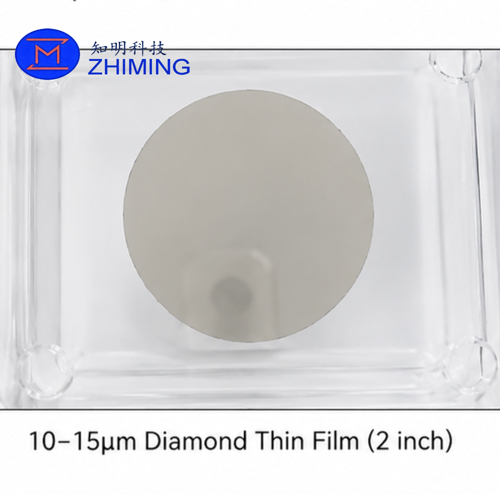
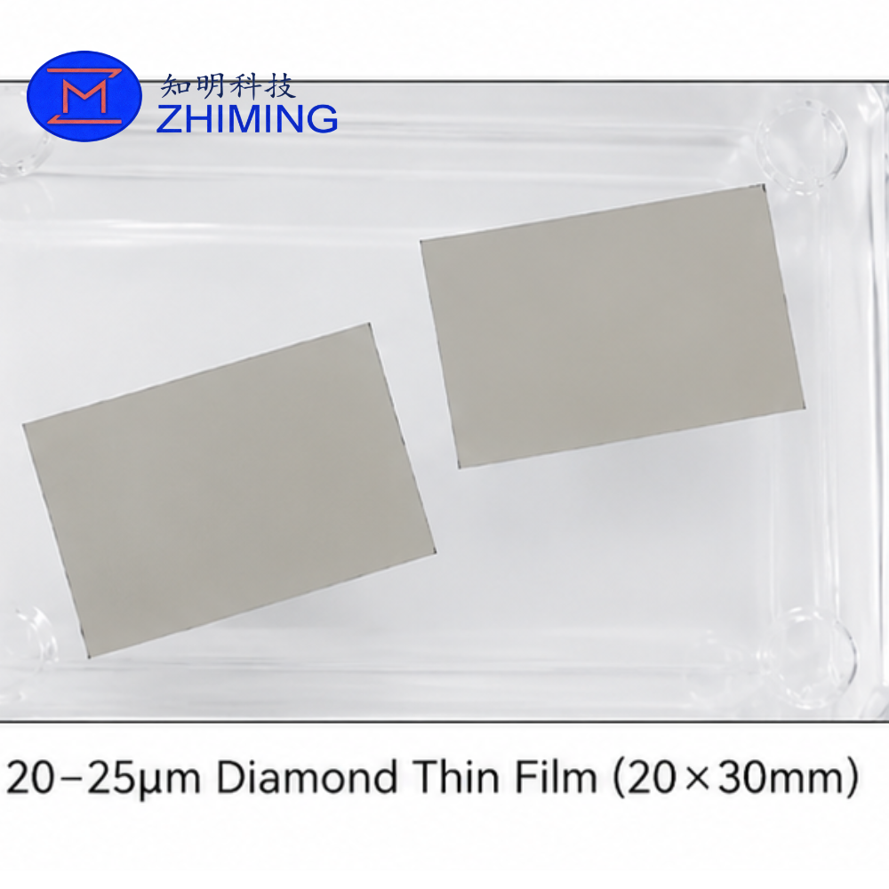
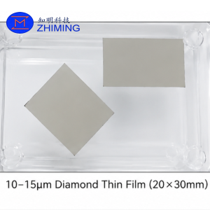
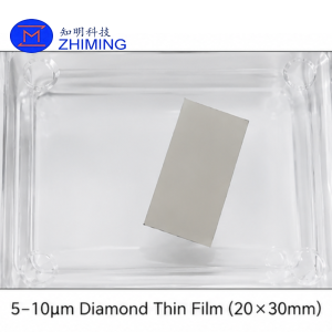
Film thicknesses are available from 5 μm to 25 μm, allowing integration into highly compact semiconductor packages where space is limited.
Self-Supporting Structure
The film does not require a silicon wafer, metal carrier, or backing substrate, reducing package complexity and interface losses.
Exceptional Thermal Conductivity
Diamond remains the industry’s benchmark thermal conductor, enabling rapid heat spreading and hotspot suppression in high-power devices.
Flexible Mechanical Properties
The ultra-thin structure provides a degree of flexibility that traditional diamond substrates cannot achieve, simplifying integration into complex package designs.
Electrically Insulating
Offers excellent electrical isolation while maintaining outstanding thermal performance, making it suitable for sensitive electronic and RF applications.
Precision Processing Capability
Supports laser cutting, customized dimensions, and application-specific geometries for advanced packaging requirements.
Especificaciones técnicas
| Parámetro | Especificación |
|---|---|
| Material | Polycrystalline Diamond |
| Estructura | Free-Standing Diamond Film |
| Espesor | 5–25 μm |
| Conductividad térmica | Ultra-High |
| Electrical Property | Insulating |
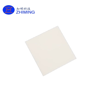
| Acabado superficial | Smooth Surface |
| Método de elaboración | Precision Laser Cutting |
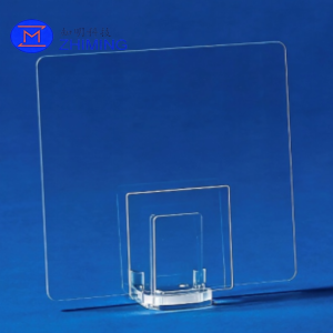
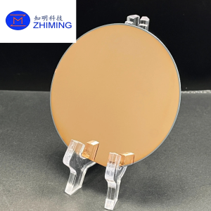
| Opciones de forma | Round, Square, Customized |
| Size Customization | Disponible |
| Application Level | Package-Level Thermal Management |
Advantages Compared with Conventional Diamond Substrates
| Propiedad | Free-Standing Diamond Film | Conventional Diamond Plate |
| Espesor | 5–25 μm | 50–500 μm |
| Peso | Ultra-Light | Relatively Heavy |
| Flexibilidad | Excelente | Rigid |
| Thermal Performance | Outstanding | Outstanding |
| Packaging Compatibility | Excelente | Moderado |
| Processability | Easy Custom Cutting | More Complex |
| Integration Freedom | Alta | Limitado |
Ámbitos de aplicación
Envasado avanzado
Suitable for chiplet packaging, heterogeneous integration, fan-out packaging, wafer-level packaging (WLP), panel-level packaging (PLP), and 3D IC technologies.
AI and High-Performance Computing
Provides effective thermal spreading for AI accelerators, advanced GPUs, CPUs, and data-center processors operating at high power densities.
Electrónica de potencia
Ideal for SiC MOSFETs, GaN devices, IGBTs, and other power semiconductor components requiring superior thermal management.
RF and Microwave Systems
Supports thermal control in RF power amplifiers, radar modules, satellite communication systems, and wireless infrastructure equipment.
Photonics and Optical Devices
Improves heat dissipation in laser diodes, optical transceivers, silicon photonics devices, and photonic integrated circuits.
Emerging Flexible Electronics
The flexible nature of the film enables thermal management solutions for wearable electronics, flexible circuits, and next-generation electronic systems.
 Capacidad de fabricación
Our diamond manufacturing platform supports:
- Free-standing diamond films from 5 μm to 25 μm
- Precision laser-cut components
- Customized dimensions and shapes
- Application-specific thickness development
- Prototype to volume production
- Strict quality control and thermal performance verification
Every film is manufactured under tightly controlled conditions to ensure uniform thickness, stable mechanical properties, and reliable thermal conductivity.
Why Choose Our Free-Standing Diamond Film?
- Ultra-thin structure as low as 5 μm
- Self-supporting design without carrier substrate
- Exceptional thermal conductivity
- Excellent electrical insulation
- Flexible and lightweight
- Suitable for advanced semiconductor packaging
- Custom dimensions and laser processing available
- Designed for future high-power and high-density electronics
Preguntas frecuentes
What makes free-standing diamond film different from diamond-coated wafers?
Diamond-coated wafers rely on a supporting substrate, while free-standing diamond film is completely self-supporting and can be integrated independently into packaging structures.
Is the film electrically conductive?
No. The film provides excellent electrical insulation while maintaining extremely high thermal conductivity.
What industries can benefit from this material?
The material is widely used in semiconductor packaging, AI computing, RF communications, photonics, power electronics, aerospace electronics, and advanced thermal management applications.
Valoraciones
No hay valoraciones aún.