
Silicon carbide (SiC) has become a material of choice in power electronics and high-frequency devices due to its high hardness, excellent thermal conductivity, and chemical stability. However, these very properties also make SiC wafers challenging to process. Cutting or dicing SiC wafers involves issues such as rapid blade wear, wafer chipping, and difficulty in maintaining dimensional accuracy, all of which directly affect yield and production cost. This article provides a comprehensive overview of SiC wafer dicing, including process principles, key parameters, and optimization strategies, serving as a technical reference for semiconductor manufacturers and equipment engineers.
1. Principles of SiC Wafer Dicing
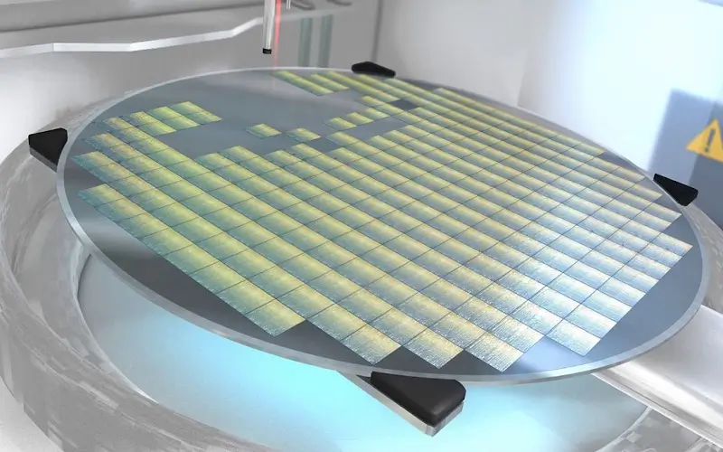
SiC wafer dicing is primarily carried out using precision dicing saws or diamond wire saws. The typical workflow includes:
- Wafer Mounting: SiC wafers are attached to a carrier wafer or tape to ensure stability during the dicing process. Proper mounting reduces vibration and prevents cracking.
- Cut Path Planning: Cutting lines and spacing are defined according to chip design specifications, ensuring post-dicing dimensional accuracy.
- Blade Motion and Cutting: High-speed rotating diamond blades or diamond wires perform the cutting. During this step, feed rate, cutting depth, and coolant flow must be precisely controlled to prevent chipping.
- Cleaning and Inspection: After dicing, wafers are cleaned, and quality checks are performed to evaluate chipping, surface scratches, and dimensional deviations.
Tip: SiC hardness is approximately 9 on the Mohs scale, second only to diamond. Therefore, blade selection and coolant strategy are critical for maintaining high yield.
2. Key Process Parameters for Yield Improvement
Proper control of process parameters is essential to achieve high-quality dicing. The following table summarizes critical variables:
| Parameter Category | Key Indicator | Recommended Range / Reason |
|---|---|---|
| Blade Selection | Blade type: diamond saw / diamond wire | Diameter 100–300 mm; diamond grit size affects surface smoothness |
| Cutting Speed | Blade line speed | 30–60 m/s; too fast causes chipping, too slow reduces throughput |
| Feed Rate | Wafer advancement speed | 0.1–0.5 mm/s; slow feed reduces stress and prevents cracking |
| Coolant | Type and flow rate | Deionized water with additives; 1–3 L/min; reduces heat accumulation and blade wear |
| عمق القطع | Depth per pass | 50–100 μm; avoid excessive single-pass depth to minimize wafer fracture |
| Vibration Control | Machine damping and stability | Reduces micro-cracks and improves dimensional consistency |
These parameters may vary slightly depending on equipment models, but the core principle is to control stress, heat, and blade wear.
3. Cutting Methods and Optimization Strategies
- Conventional Dicing Saw
- Advantages: High precision, suitable for small chips
- Disadvantages: Rapid blade wear; high chipping risk on SiC
- منشار سلك الماس
- Advantages: Lower cutting stress, suitable for large wafers (6-inch to 12-inch)
- Disadvantages: Higher equipment cost; operator skill required
- Laser-Assisted Dicing
- Advantages: High precision for ultra-thin or special wafers
- Disadvantages: Expensive equipment and operational cost
Optimization strategies include:
- Selecting cutting method based on wafer size and material hardness
- Controlling diamond grit size and feed rate precisely
- Using high-flow coolant to minimize thermal stress
- Regularly monitoring and replacing worn blades
4. Practical Case Study
A semiconductor manufacturer applied diamond wire saws with controlled feed rates and high-flow deionized water coolant to dice 6-inch SiC wafers. The wafer yield improved from 85% to 96%, and blade lifetime increased by 30%. This example demonstrates that systematic control of key parameters can significantly reduce chipping and improve overall production efficiency.
5. Challenges and Considerations
Despite these improvements, several challenges remain in SiC wafer dicing:
- الإجهاد الحراري: Excess heat can cause micro-cracks, requiring precise coolant flow and temperature management.
- Blade wear: High hardness accelerates wear; monitoring blade condition is crucial.
- Dimensional precision: SiC wafers for high-power devices demand tight tolerances (<10 μm).
- Cost vs yield: Optimizing dicing parameters involves balancing production cost with wafer yield.
Addressing these challenges requires an integrated approach combining equipment selection, process parameter optimization, and real-time monitoring.
6. Conclusion
SiC wafer dicing is a critical step in producing high-quality power electronics components. Achieving high yield requires careful selection of blades, precise control of feed rate and cutting depth, effective coolant management, and vibration reduction. When properly implemented, these measures can reduce wafer breakage, extend blade life, and improve overall production efficiency.
⚡ Want to discover the optimal SiC wafer dicing solution for your production line?
Contact us today for customized quotes and technical support!